[Date Prev][Date Next][Thread Prev][Thread Next][Date Index][Thread Index]
Re: VXS & Signal Distribution (fwd from Ben Raydo)
---------- Forwarded message ----------
Date: Thu, 13 Mar 2008 16:18:36 -0400
From: Benjamin Raydo <braydo@jlab.org>
To: Gerard Visser <gvisser@indiana.edu>,
Ed Jastrzembski <jastrzembski@jlab.org>
Cc: Fernando J. Barbosa <barbosa@jlab.org>, C. Cuevas <cuevas@jlab.org>,
Hai Dong <hdong@jlab.org>, Jeff Wilson <wilson@jlab.org>, agupta@jlab.org,
halld-electronics@jlab.org
Subject: Re: VXS & Signal Distribution
Gerard/Ed,
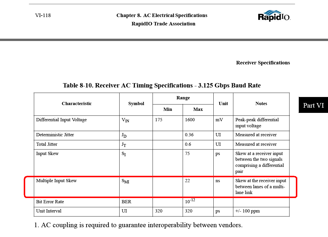
The attached image may be of use for tomorrow's discussion (this is the skew
spec referenced by VITA 41.2/VXS). Doesn't say much other than that we must
manually measure pair-to-pair skew on each slot of the backplan if we are to
guarentee a setup relationship between trigger and clock. I think the large
pair->pair skew (22ns max) in the spec comes from fiber links that
eventually get translatted into VXS copper pairs (I don't see how such a
large skew can develop on our "small" 20 slot backplane alone).
Have fun,
Ben
----- Original Message -----
From: "Gerard Visser" <gvisser@indiana.edu>
To: "Ed Jastrzembski" <jastrzembski@jlab.org>
Cc: "Benjamin Raydo" <braydo@jlab.org>; "Fernando J. Barbosa"
<barbosa@jlab.org>; "C. Cuevas" <cuevas@jlab.org>; "Hai Dong"
<hdong@jlab.org>; "Jeff Wilson" <wilson@jlab.org>; <agupta@jlab.org>;
<halld-electronics@jlab.org>
Sent: Thursday, March 13, 2008 3:03 PM
Subject: Re: VXS & Signal Distribution
> Hi Ed,
> I could make the phone meeting tomorrow at 10am if it is still on -
> please consult with Fernando and let me know. (You guys can write me at
> 9am, that is warning enough!) Fernando tentatively indicated it would
> get rescheduled... Better to proceed if possible I think.
> I think this discussion should proceed on our mailing-list (I am
> attaching your original document here for the benefit of other readers).
> I read your document, a block diagram might make it a little clearer
> but I think I understand what you are proposing. However, I'm afraid I
> don't quite agree with the plan.
> You propose that the SD module resync the 3 trigger bits to the
> outgoing half-crate clock [good] but then you go on to skew them in two
> different ways: First, you intend to use LVDS for the trigger bits and
> LVPECL for the clock. _Why_ _not_ just use LVPECL for everything? (Same
> question I've asked before...) Second, you intend to skew the various
> clock lines on the SD board to compensate for the slot-slot skew on the
> backplane [I don't see why we care about slot-slot skew], but _why_
> _not_ then also skew the trigger lines on the SD board. As it is, your
> slot-clock-deskew scheme introduces a skew between clock and trigger
> bits within 1 slot. You add a "requirement" that the front-end boards
> deskew it if necessary. Well, I don't have any room for delay chips,
> etc., and while I could maybe use the FPGA DLL blocks to deskew, it's a
> pain I intend to avoid. I am not providing any such deskew feature, the
> ADC125 expects the trigger bits to have a particular, well-defined,
> universal timing specification for _example_ as follows:
> "The trigger bits shall be valid 0.5 ns after the rising edge of the
> clock and held valid until 0.0 ns after the next rising edge of the
> clock."
> However, I agree that I only require about a 3 ns window to capture the
> trigger bits (I am doubling the "1.5ns" figure to be conservative). So,
> if you wish to implement the (within-slot) skew-introducing mechanisms
> described, it is ok as long as you can guarantee me some fixed 3 ns
> window. I would prefer to, for example, simply capture the trigger bits
> on the falling edge of my received clock, but I will implement one
> (universal) phase shift as required to put the capture point anywhere in
> the 8 ns cycle, as long as you can specify it ~now. I don't know what
> the backplane slot-slot skew in VXS is (this is in the spec, right?), if
> it is <3 ns or so I suppose it will be possible for both of us to have
> our way.
> On the other hand, I think a better approach would be as follows:
> -A- Fanout your clock
> -B- Use trace delay (as you say, it's low jitter) to deskew the slot
> clocks that result (in "D" below).
> -C- Fanout 1:2 each of these
> -D- One goes to slot clock line directly
> -E- One drives the clock of three 'EP52's or equivalent
> -F- The 'EP52's drive the slot trigger lines directly
>
> To clarify a few other points:
> 0. Reset is just another trigger bit. The trigger distribution (and
> trigger receiver hardware in front end boards) should not preclude any
> possible encoding different commands into the bits. With 3 lines you
> could have 3 trigger commands (one-hot encoding), or 7 trigger commands
> (binary excluding 000 as a NOP), or more by serializing. Yes maybe
> you're "sure" you'll never need more than 3 even 10 years from now.
> Still, the fixed hardware, I mean boards not FPGA firmware, ought to not
> care about the meaning of these bits. Probably this is true of your plan
> for the TI and SD, I don't know.
> 1. I don't at all understand why the slot-slot clock skew is a big
> deal. The signal cables (at least for the ADC125 and F1TDC for FDC) will
> have a few ns of skew. Even for the ADC250, the only detrimental effect
> of clock skew would be to misalign the timing of signals in the energy
> sum... but no doubt there has to be some way of adjusting the timing of
> different channels and modules (by integer clock ticks) to get the
> energy sum to work right anyway... Isn't that true? The only other
> effect of clock skew is to change the "t0" calibration offset for each
> channel, that's ok, there has to be some calibration offset anyway...
> 2. Yes the ADC125 will have the geographical address pins connected so
> the GA is available to the VME interface FPGA. I don't intend to send it
> out to my other FPGA's in particular the one that does the trigger and
> data processing function. I _could_ of course, I just don't intend to at
> this time.
> 3. When you say the busy signal is "LVDS, positive asserted" I take it
> as an affirmative answer to my question that DP29+ > DP29- is the
> assertion of busy, DP29+ < DP29- is the negation.
> 4. I still have question now how does the TI take the incoming trigger
> information and break it down into commands for modules at 250, 125, and
> 31.25 MHz clock rates... Are you implying that there is a 32 ns deadtime
> in the trigger system, i.e., that the ADC125 will _never_ be triggered
> on back-to-back cycles or in fact never triggered less than 4 cycles
> after a previous trigger. This would be useful information, I've
> inquired before about it but to my knowledge I haven't heard a
> definitive specification. I am assuming still the ADC125 may be
> triggered on two consecutive cycles, but I suppose then the ADC250 will
> never be, and I don't understand how the F1TDC's are to handle that.
>
> Well, we can discuss further tomorrow. It's good that we're getting
> these important details sorted out, and I must apologize if I'm being
> too pushy here but I think it is important that the plan is thoroughly
> understood, and that it also does not just push issues from one side of
> a "fence" to another.
> Sincerely,
>
> Gerard
>
> Ed Jastrzembski wrote:
>> Hi Gerard,
>> Attached is a brief description of our ideas about signal
>> distribution at the crate level. I'm looking forward to hearing your
>> comments tomorrow.
>> -Ed J.
>>
>>
>> Gerard Visser wrote:
>>
>>> Hi Fernando, Ed,
>>> Sounds good - I'll look forward to reading that.
>>> Next friday at 10 is fine with me, I have another meeting at 11am,
>>> but it's good to have a time limit anyway :)
>>>
>>> - Gerard
>>>
>>> Fernando J. Barbosa wrote:
>>>
>>>> Hi Gerard,
>>>>
>>>> I talked to Ed and he will be sending you an email outlining the
>>>> architecture of the signal distribution chain. We have talked in the
>>>> past about parts of the system but it is best to put it all in
>>>> perspective. Actually, this will serve us well as a brief review,
>>>> especially in light of the main readout modules that use the VXS
>>>> crates.
>>>>
>>>> Additionally, I would like to suggest that we have a conference call
>>>> next Friday at 10:00 a.m. (EST) to go over the VXS signal distribution
>>>> and its impact on board resources, delays, etc. Please let me know if
>>>> this works for you.
>>>>
>>>> Thanks,
>>>> Fernando
>>>>
>
VXS_RapidIOLaneSkew.PNG